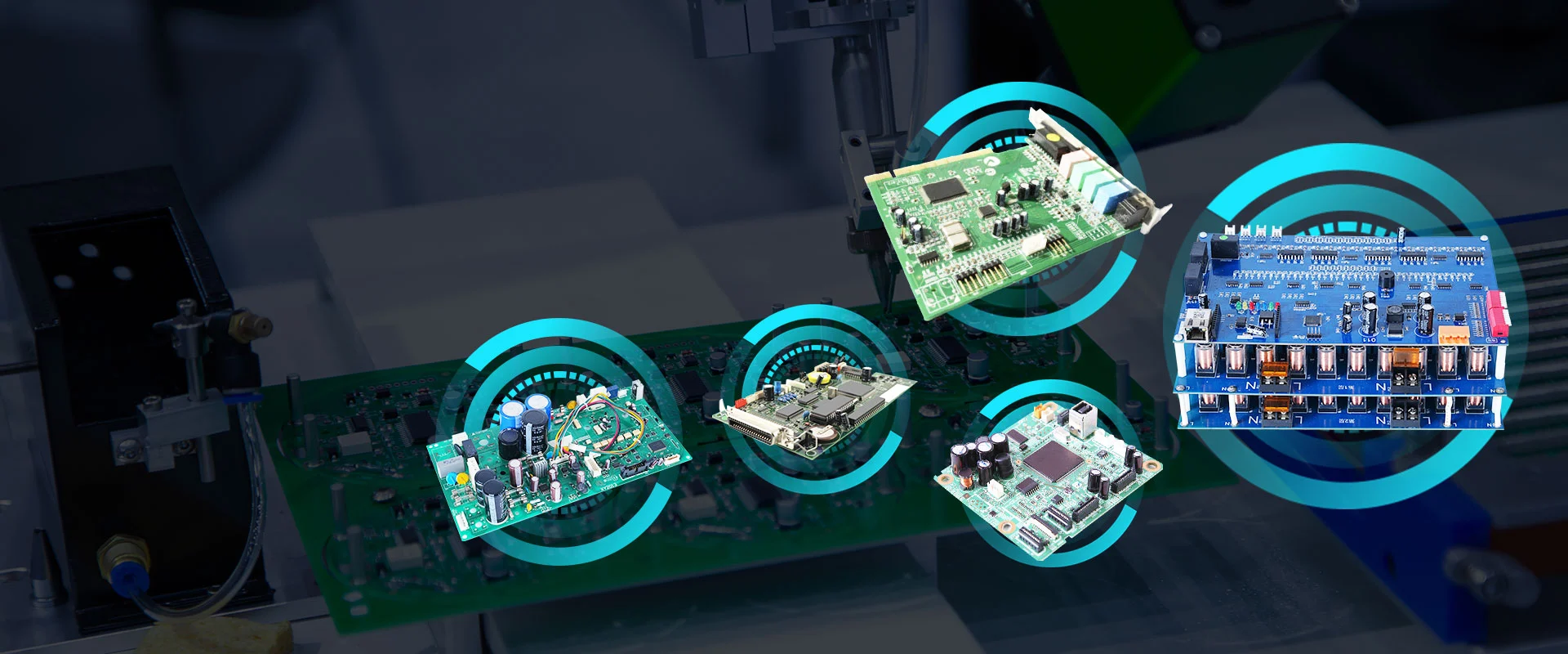

Printed Circuit Board (PCB)
Every electronic device relies on a precisely manufactured printed circuit board (PCB). With over 12 years of experience in PCB fabrication, assembly, and testing, Fanway delivers high-performance solutions for automotive, healthcare, consumer electronics, and industrial automation. From prototypes to bulk production, we ensure your boards meet strict quality and reliability standards.
Fanway’s Advanced PCB Solution Including:
From 1-32 layer designs with 4/4mil trace/spacing, HDI, and blind/buried vias.
Various Materials: FR-4, Rogers, aluminum, ceramic, flexible, and rigid-flex PCBs.
Surface Treatment: ENIG, HASL, OSP, and gold plating.
Fast Turnaround and Cost-Effective
Our Prototype delivery in 48 hours, 1000pcs orders in 5 days.
We have DFM analysis free of charges to minimize design errors.
Quality Control
100% electrical testing and AOI inspection.
Compliant with IPC, UL, RoHS, and ISO 9001 standards.

| Layer | Up to 108L |
| PCB Thickness | 0.5-17.5mm |
| Min. Mechanical Hole Dia & Min. Laser Hole Dia | 0.1mm & 3mil |
| HDI Type | 1+n+1/ 2+n+2/ 3+n+3 |
| Min. Line & Track Width | 3/3mil |
| Impedance Control | +/-5% |
| Max Copper Thickness | 12oz |
| Max Board Thickness Hole Dia. Ratio | 18:1 |
| Max Board Size | 650 x 1130mm |
| PCB Material | FR4/ Hi-Tg/ Rogers/ HALOGEN Free/ RCC/ PTFE |
PCB Work Flow
Shenzhen Fanway Technology Co., Ltd
Office Add: F601, Industrial Building of Hengtai, Tangkeng Road, Guantian Community Shiyan Street, Bao'an District, Shenzhen, Guangdong, China, 518108
Factory Add: F2, Building 3, The First Industrial Zone of Mingjinhai, Shiyan Street, Bao'an District, Shenzhen, Guangdong, China, 518108
E-mail: karena@fanwaypcba.com
Cell: +8615013656200
Copyright © 2025 Fanway | All Rights Reserved.