
Complex HDI PCB Manufacturing
Complex HDI PCBs (High-Density Interconnect) provide higher wiring density compared to standard PCBs, it enable a smaller, more compact, and high-performance electronic designs.
The Feature of HDI PCB:
Finer trace widths and spacing achieve more connections in a smaller area.
Microvias (<150µm diameter) reach high-density interconnections.
Blind & buried vias improved signal integrity and reduced board size.
High layer counts (20+ layers) support for complex circuit designs.
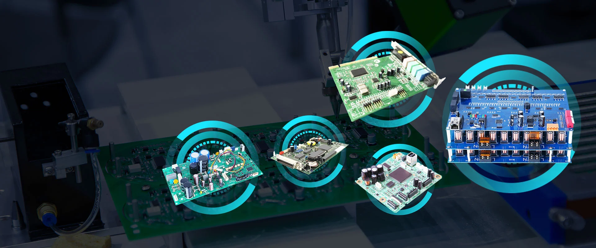
As an experienced complex HDI PCB manufacturer, Fanway delivers precision engineered solutions for industries including medical devices, automotive systems, 5G telecommunications, AI hardware, and advanced electronics. Our capabilities ensure fast turnaround times and cost-effective production with high quality.
Why Choose Us?
✔ Strict quality control with AOI, X-Ray, and electrical testing to guarantee PCB reliability.
✔ Competitive pricing to optimize supply chain and efficient production reduce costs.
✔ Fast delivery with real-time order tracking ensures on-time completion.
✔ Technical expertise by full support from design to final production.
HDI PCB Technology Classification
|
Technological Class |
Structure |
Complexity |
Applications |
|
HDI Class 1 |
1+N+1 |
Low |
Basic consumer electronics, simple devices |
|
HDI Class 2 |
2+N+2 |
Medium |
Advanced consumer electronics, automotive |
|
HDI Class 3 |
3+N+3 |
High |
High-performance devices, 5G, AI systems |
|
HDI Class 4 |
4+N+4 |
Extremely High |
Cutting-edge applications, semiconductor |