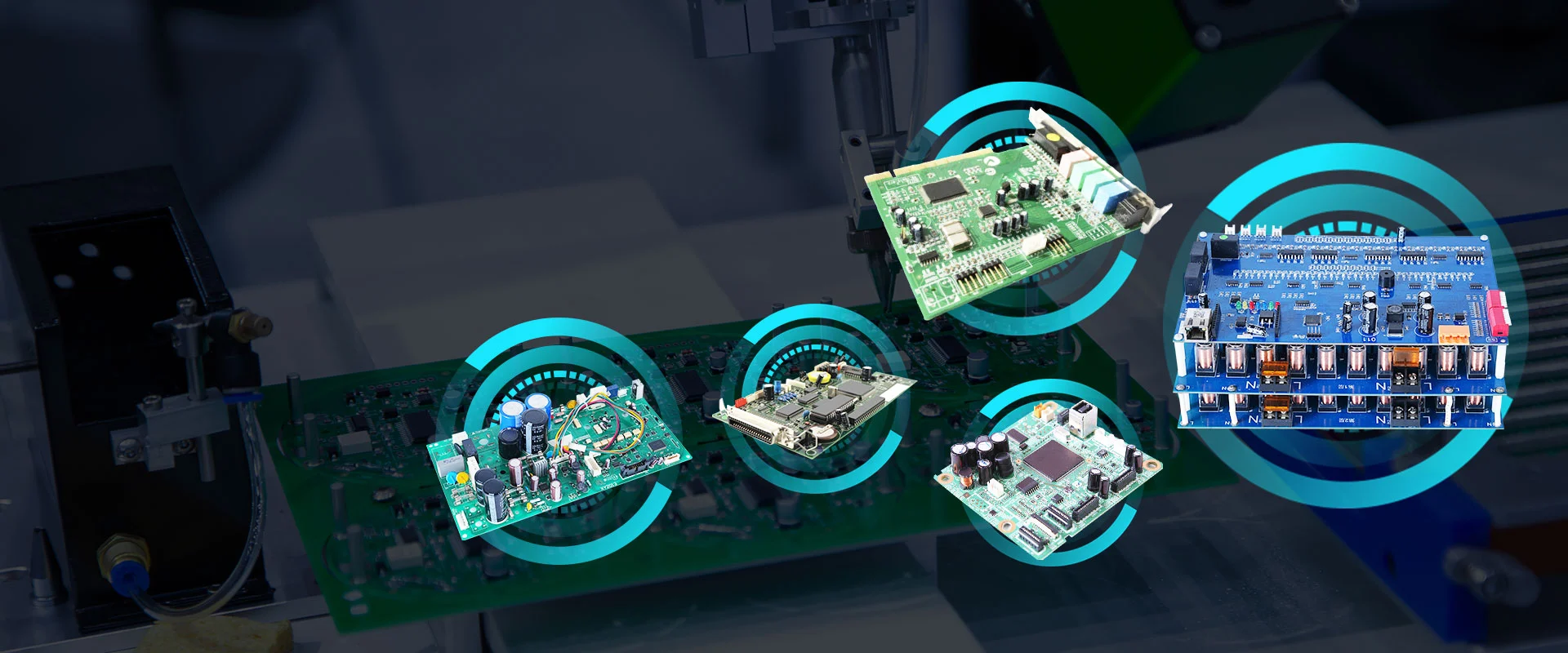

PCB Design and PCB Layout From Concept to Production
Fanway provide complete PCB design and layout solutions, converting your concepts into reliable, high performance circuit boards. With 12+ years of experience and 500+ projects completed, we deliver defect-free designs for industrial controls, automotive systems, medical devices, 5G & RF modules, and IoT technologies.
Why Partner with Us?
1. Expert Design
Tailored Analysis: Custom layer stack-ups (1-32 layers) and materials selected for signal integrity (≥10GHz), thermal performance, and budget.
Rigorous Testing: Signal integrity (SI), power integrity (PI), and EMI/EMC validation using Cadence Allegro and Mentor Xpedition, addressing 90% of design risks early.
Manufacturing Focused Design: IPC-610 compliance to minimize production defects by 30-50%.
2. Optimized Layout Solutions
High-Density Interconnects: 0.1mm micro-vias, 3/3μm trace/spacing for compact 5G and wearable devices.
Heat Management: Custom copper thickness (1-10oz) and thermal via arrays to reduce hotspots by 40%.
EMC Assurance: Shielded layers, ±5% impedance control, and grounding strategies for FCC/CE compliance.
3. Full-Cycle Support
Fast Turnaround: Initial design draft in 48 hours.
Cost Efficient BOM: Component lifecycle management to reduce procurement costs by 15-30%.
Production-Ready Output: Gerber files, assembly drawings, 3D models, and clear manufacturing guidelines.
Clear Process
Requirement Review → 2. Schematic Design & Testing → 3. Layout & Routing → 4. DFM/DFA Checks → 5. File Delivery → 6. Production Support