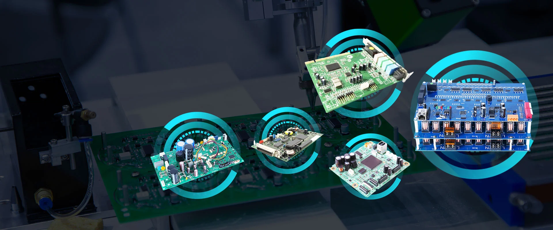

Multi-layer PCBs is a PCB that integrate three or more conductive layers with insulating materials, enable compact, high-performance electronic designs. These boards could support complex circuitry through advanced interconnection technologies including blind vias, buried vias, and through-holes.
Fanway specialize in fast-turn multi-layer PCB production, and delivering high quality boards at competitive pricing and fast delivery.
The Benefits of Multi-layer PCBs
Compact Circuit Integration – Multiple layers allow higher component density in limited space.
Enhanced Signal Quality – Dedicated power/ground layers minimize EMI and crosstalk.
Improved Thermal Performance – Built-in heat dissipation layers increase reliability.
Space & Weight Savings – Reduces external wiring for lighter, smaller devices.
Design Flexibility – Supports high-speed, RF, and power applications.
Our Capabilities
● Layer Options from 3 to 108 layers.
● Materials include FR4, Rogers, metal-core, and other high-frequency substrates.
● Features with blind/buried vias for high-density routing, HDI technology with microvias (<150µm) and tight impedance control (±8%).
● Surface finishes include ENIG, HASL, OSP, immersion silver, gold plating
● Quality assurance by AOI, X-ray inspection, electrical testing.
Industries We Serve
Telecommunications
5G infrastructure, network equipment
Automotive
ADAS, infotainment, control modules
Medical
Diagnostic imaging, patient monitoring
Industrial
Power systems, automation controls
Aerospace/Defense
Avionics, radar systems